


It has become a usual sight to see anyone, young and old alike, is readily able to record moving images, using their smartphones, to capture anything from an ordinary scene from their day to special occasions such as holidays, sports day at school and weddings.
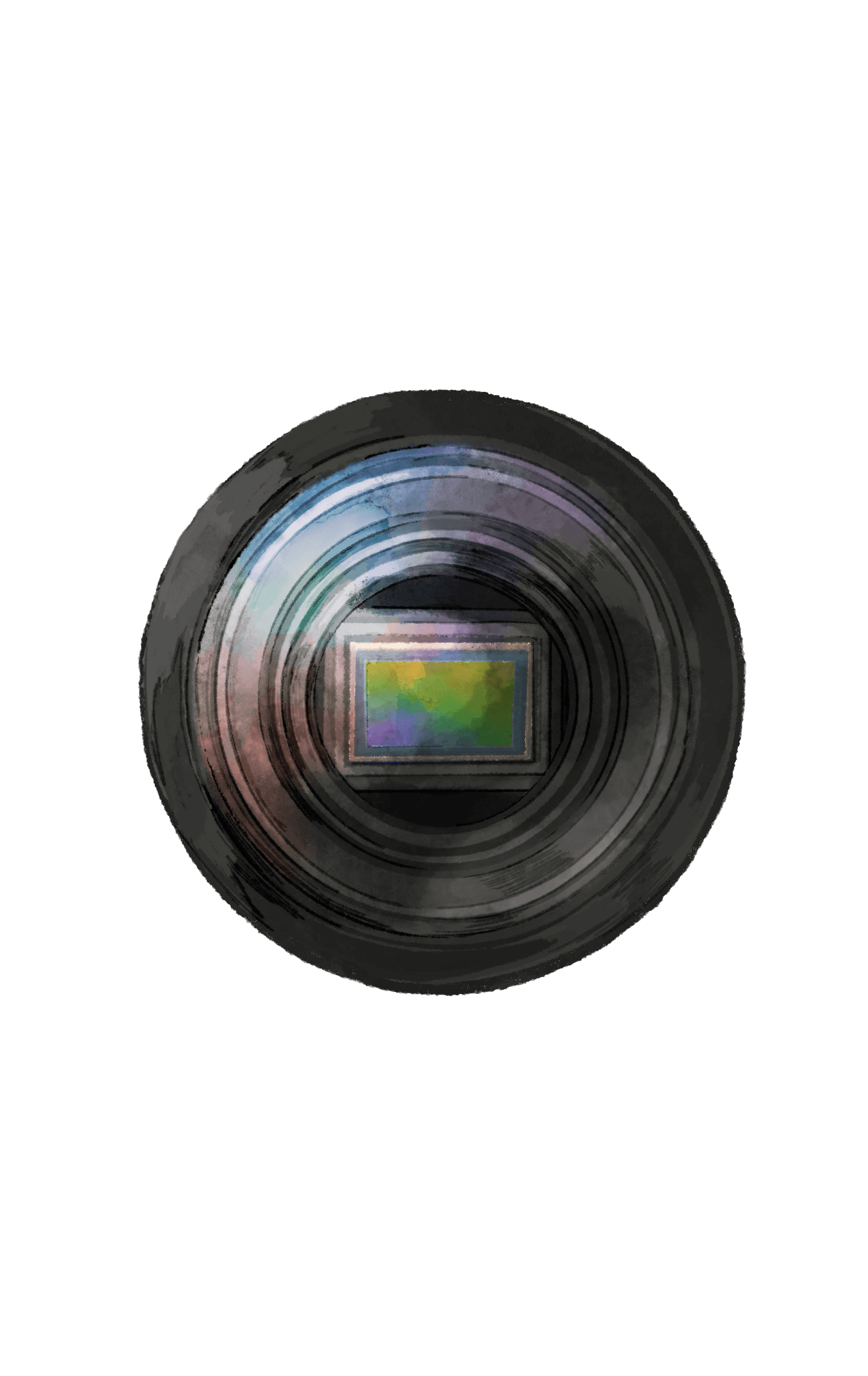
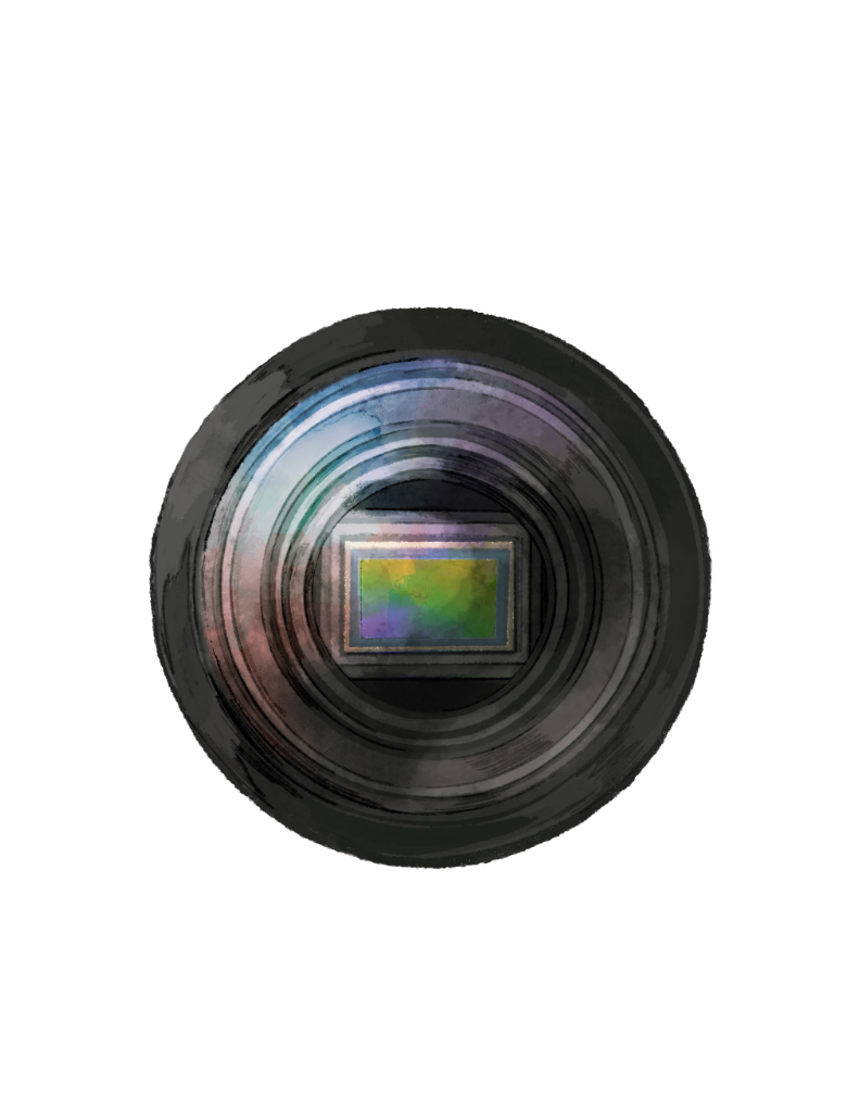
Today, we can use this small device at hand to capture those special moments in a video and share it with a few finger taps. It is image sensors that make all this possible. This device, a semiconductor, functions like the retina in the human eye. It captures the light that comes through the camera lens and converts it into electrical signals to form a digital picture.
The history of Sony’s image sensors is a story of struggles, successes and evolution. In 2012, precisely 10 years ago, a page was turned by the invention of our “stacked CMOS image sensor.”
The structure unique to this revolutionary stacking technology enabled to realize smaller image sensors with higher image quality and functionality. Today, about 90% of image sensors by Sony adopts this stacking technology. The technology has also given birth to many ground-breaking image sensors.
Before going into detail of how the stacking technology was developed, let’s take a look at how Sony entered the image sensor market in the first place to understand why we make these devices.

The stacked CMOS image sensor is prevalent in society today, with smartphones being the most recognizable example. The history of image sensor development at Sony goes back more than half a century.
We initially found great potential in CCD as an electronic “eye” and, in spring 1970, started our research and development of image sensors, which still continues today.
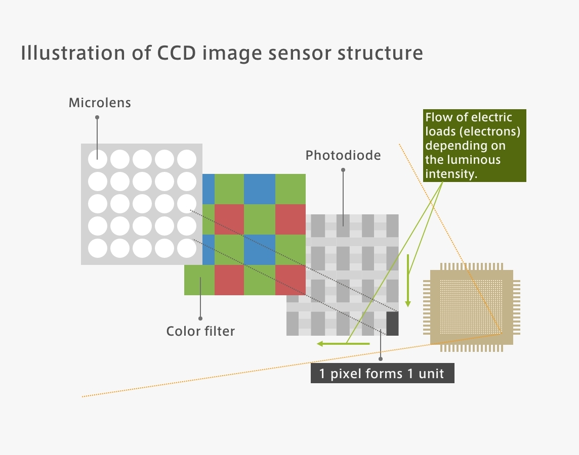
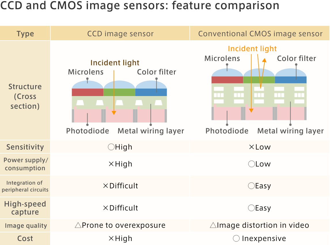
The Company first developed a CCD image sensor. CCD stands for charge-coupled device, an original form of semiconductor in which devices known as pixels passed electric charges (electricity) as electrical signals from one pixel to the next like the water bucket relay game. We wanted to adapt the semiconductor into an image sensor which converted incident light into electrical signals, which formed a digital image. Thus, our R&D efforts started.
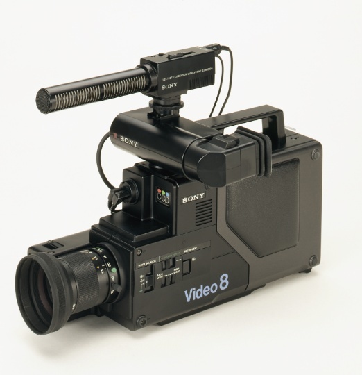
Inexpensive CCD image sensors would realize inexpensive video cameras so that they would be accessible and affordable even to ordinary people. This idea was the drive behind our projects, which first led to a successful launch of a CCD image sensor, ICX008, in 1978. This world’s first CCD image sensor was adopted in a CCD color camera mounted on a Japanese airline ANA’s jumbo jet. Passengers were thrilled to see the real-time images during a take-off and landing. Dedicated efforts continued by the development and manufacturing teams to improve the production yields, and in 1985 we successfully created the CCD-V8, our consumer 8mm video recorder with a built-in camera.

Four years later in 1989, an 8mm camcorder, CCD-TR55, stirred a sensation in the market for its advanced features and smaller size, launched under a copy of “a passport-size camcorder.” This success lifted Sony to the leading position in the image sensor industry.


Though leading the CCD image sensor market, Sony made a critical decision to change its direction toward CMOS image sensors.
CMOS, or complementary metal-oxide semiconductor, is another type of image sensor that combines each pixel with the mechanism to convert electric charge to electric voltage and amplify them (amps).
Compared to CCD, which forwards the electric signals in a relay, CMOS can transmit the signals much faster due to its structure. Moreover, it works on lower voltage and consumes less power. It was CMOS image sensor that better suited for movies and high-definition imagery. The drawback with the CMOS image sensor was the signal’s susceptibility to noise, as the noise generated in each pixel was amplified concurrently with the signals.
The year 1996, when Sony was in its early days of developing CMOS image sensors, saw a gradual diffusion of liquid crystal displays(LCD) corresponding to the rise of the internet and high-vision broadcasting. Keeping a close eye on the trends, we believed that CMOS image sensor would be an unavoidable choice in the future.
Sony was one of the last to join the development of CMOS image sensor, but was aware that a decision had to be made, before it’s too late, to change the course dramatically toward CMOS image sensor to remain ahead of the game in the image sensor market. So, we discontinued the investment in augmenting the production of CCD image sensors in 2004 and, instead, built momentum of the investment in the development of CMOS image sensors.

Sony started gradually launching CMOS image sensors in year 2000, but the images produced by the device lacked brightness and were prone to noise. The CCD image sensor was still a mainstream choice to be implemented in products such as digital cameras and camcorders for its high sensitivity and better image quality.
The fundamental problem with the CMOS image sensor was with its basic structure. The device had a metal wiring layer, which conveyed electrical signals, on top of a photodiode to convert light into electrical signals. The major drawback of this structure was that the incident light was blocked by the wiring layer, compromising the device’s sensitivity.
Sony’s engineers thought, “the light blockage can be avoided if we put the photodiode closer to the incident light.” ―― They saw potential in the idea of taking in the light from the reverse side of the sensor to capture light more efficiently. The idea of a back-illuminated structure had existed in the industry for over 20 years previously, but it was never realized due to its radical difference from the conventional systems for manufacturing semiconductors.
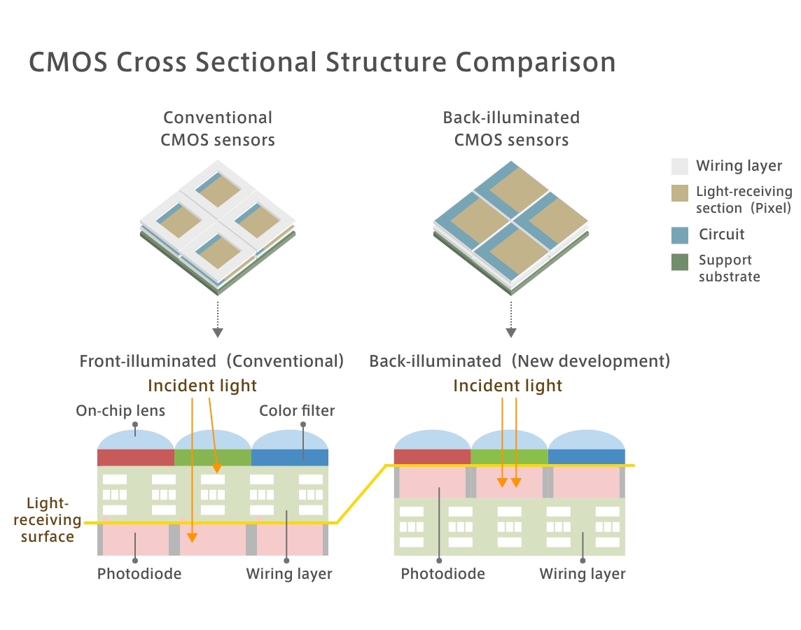
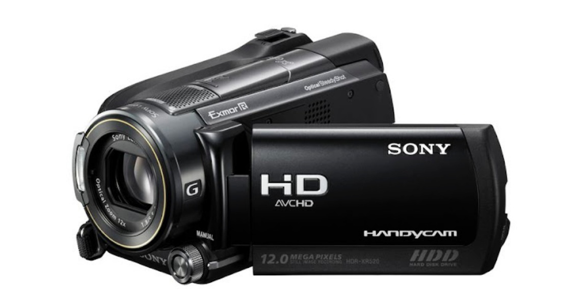
Thus, a project started in 2002 to realize a back-illuminated CMOS image sensor. After long 7 years of unspeakable cycles of trials and errors, a back-illuminated CMOS image sensor was brought to mass production in 2009 for the first time in the entire world. The first products that implemented this brand-new image sensor were the digital high vision camcorders, or “Handycam,” HDR-XR520V and HDR-XR500V.
Sony’s back-illuminated CMOS image sensor, commercialized before its competitors, stirred a sensation in the industry for the beautiful, bright and low-noise images it created.
Meanwhile, Sony’s semiconductor team already had their eyes on the next goal. It was to implement the back-illuminated CMOS image sensor in a mobile phone camera. They embarked on this mission when a seasoned engineer joined the team. He later became a key person to make a great leap for Sony’s CMOS image sensor into next generations.
His name is Taku Umebayashi, and he would subsequently bring the stacked CMOS image sensor into the world.
