


The stacked CMOS image sensor has become Sony’s flagship product that keeps the Company’s image sensor business going. Developed and successfully commercialized by Taku Umebayashi, who was decorated with the Medal with Purple Ribbon, and other engineers, taking more than four years, this image sensor boasts the largest market share globally in the mobile business and is installed in many smartphones across the world.
What’s more, the stacked structure is proving its value beyond the mobile business, expanding the scope of its applications to the image sensors in other areas. Today, it is the widely used technology in the domain of sensing for data applied, for example, in autonomous driving technology, factory automation in manufacturing, and digital transformation (DX) in retail.
Sony’s image sensors were born and developed driven by various aspirations and ambitions of the Company’s engineers, who wanted to “keep memories in clear images” or “create an imaging culture.” The tradition was passed on through generations of semiconductor engineers and led to the stacked CMOS image sensor, realized by Taku Umebayashi and his team. This image sensor already surpasses the human eye in some areas and is dramatically changing people’s lifestyles. Moreover, it is expected to become an important element of the social infrastructure of a new era to come.
The secret weapon of the stacking technology is that it has created more options for image sensors. Why is this so important? This concluding story of the series reveals the diverse values and possibilities the stacked CMOS image sensor offers to society.

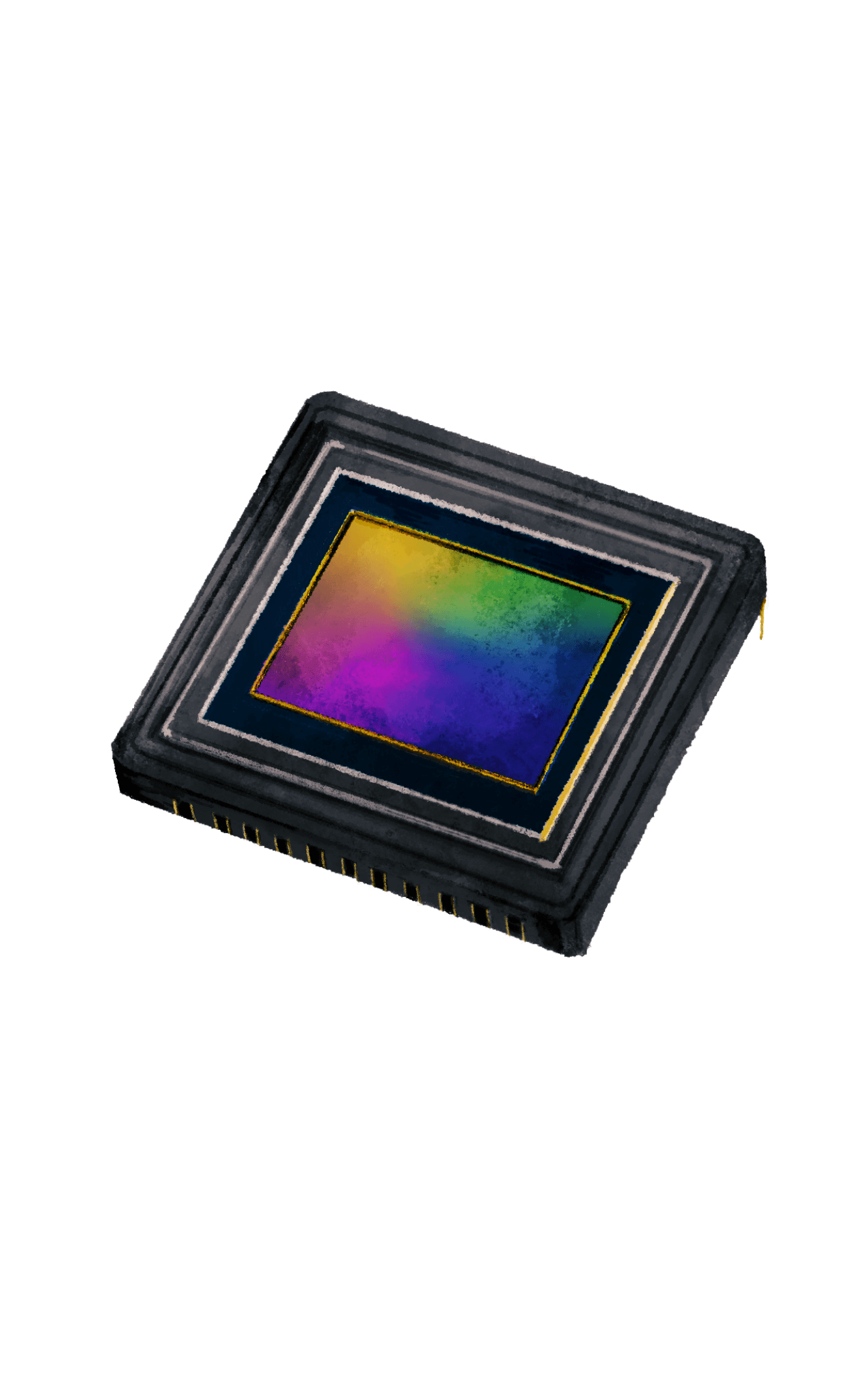
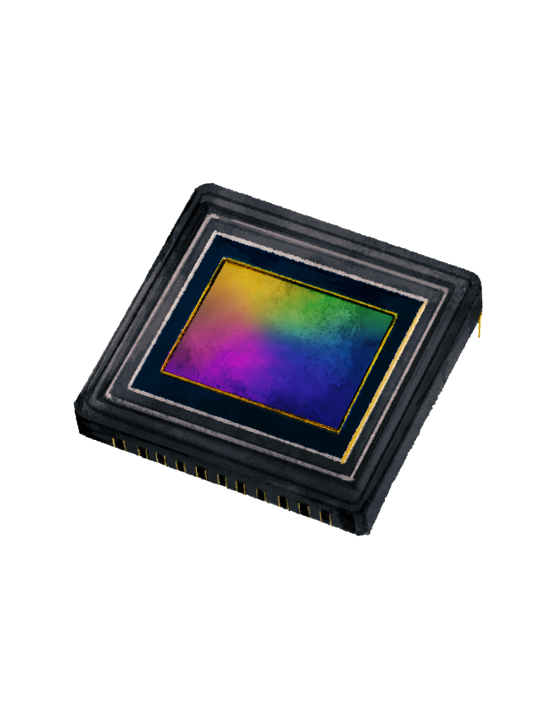
The true value of the stacked CMOS image sensor cannot be explained without mentioning the Cu-Cu (copper-copper) connection technology, which Sony developed in 2015. While the stacked CMOS image sensor achieved both smaller sizes and enhanced capabilities in image sensors, the Cu-Cu connection technology was the behind-the-scenes enabler, facilitating even smaller image sensors with more features as well as the enhanced productivity.
This technology is used to connect the pixel chip and logic circuit chip of a stacked CMOS image sensor. Electricity is conducted through the connected Cu (copper) terminals formed on the surfaces of the chips. Before this technology, the two chips had to have the areas reserved for a device known as a through-silicon via (TSV), which penetrated the chips to connect them in order to pass electricity from one to the other.
In the 2000s, various research institutions and corporations studied Cu-Cu connections, but it was Sony that became, in 2015, the first in the world to succeed in establishing mass-production technology for Cu-Cu connection. Removing the need for the area reserved for the TSV enabled to reduce the device size. The freed-up area also meant more design flexibility and higher integration intensity of diodes. In other words, this novel connection made a breakthrough in the stacking technology and opened up a whole new possibilities for image sensors.

by SWIR image sensors

The stacked CMOS image sensor advanced by the Cu-Cu connection— what is the value it offers to society and for the future?
The remarkable advantage of the stacking technology is in the two-tier structure of the pixel and logic circuit chips, which enables more flexibility in the circuit design, facilitating the selection of features to implement as the intended application requires. Realizing high-speed, more capabilities, and lower power consumption and manufacturing cost, the stacked CMOS image sensor can provide an ideal platform as technology that offers more possibilities for product development to meet specific application requirements.
What value does this platform offer in each of the Mobile, Automotive, Industrial and Solution areas?
First off, in the Mobile area, the stacking technology is said to be the enabler of the immense advancement made in smartphone cameras.
For example, someone who is not a professional photographer may shoot amazing photos and movies today using a small, slim mobile device, thanks to the features like the 4K imaging, high dynamic range imaging for high-contrast scenes, and AF (autofocus) tracking that automatically keeps a focus on the target even when it is in motion. Today’s smartphones are also equipped, in their compact and slim bodies, with several cameras, from a large aperture to telephoto cameras. This is all thanks to the stacking technology, which has enabled to ultimately minimize the image sensor size, leading to small, high definition, cameras with enhanced capabilities.
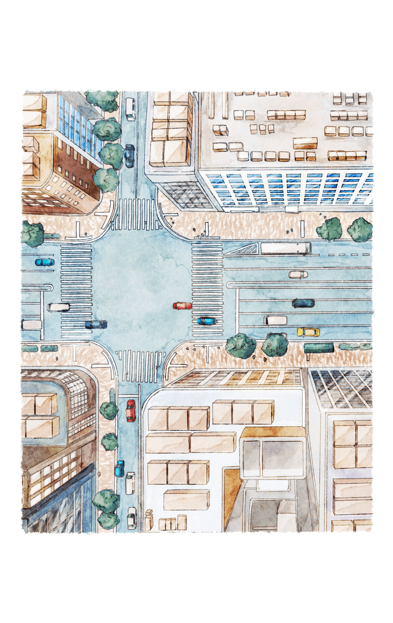
To keep up with the progress in the technology in mobility, such as advanced driver-assistance systems (ADAS) and autonomous driving (AD), the image sensors for automotive use face growing demand for greater performance than the human eye can deliver, in accurately sensing longer distances even under demanding conditions such as reduced luminance in the evening, backlit settings near tunnel exits and dark passageways at night. The stacking technology makes a significant contribution to realizing the high resolution necessary for clearly capturing images of far-away objects and the sensor size that does not compromise the vehicle design. The separated circuit section allows more options for selecting optimal generation of process to realize the features required in the automotive applications. This has also increased the possibilities toward enhancing the performance of the image sensors for automotive use.
Now, let’s take a look at the IMX500 intelligent vision sensor, which integrates AI processing capability into the stacked circuit section. Launched in May 2020, this world’s first intelligent image sensor can implement the AI processing according to the intended purpose—an ultimate device that has both the retina and brain directly connected in a single chip. Today, the growing trend in DX is driving the use of cloud servers to process a multitude of data uploaded from the IoT devices. However, the capacity this method offers is said to be finite. Meanwhile, IMX500 only outputs semantic information (metadata) generated through AI processing in the image sensor. Compared under a set of assumptions, the data volume shrinks to 1/7400 that of a conventional image sensor, significantly reducing the data volume to be transmitted to, and processed by, the cloud servers. This also has a potential advantage to lower the power consumption on the cloud side required for its system maintenance. It is also advantageous in terms of addressing privacy, since the metadata is removed of the information that can identify people.
Various trial projects involving IMX500 are already underway in society, including the City of Rome addressing its social issues such as inner-city traffic congestions, as well as the introduction of smart technology at diverse commercial premises and trials of smart building projects.


Now we turn to the image sensors for industrial use. The trend for automation and reduction of manpower is gaining impetus in the industrial area, notably in manufacturing and logistics. There is growing demand that image sensors, that determine the camera performance, deliver accurate capturing of information that are indiscernible by the human eye. Among the diverse image sensors with unique attributes Sony offers to the industrial sector, the SWIR (short wavelength infrared) image sensor is a treasure trove of Sony’s technology and expertise, including the stacking technology. Operating in the SWIR light range can facilitate the inspection tasks that are hard to perform with a naked eye, such as sorting different types of materials, inspecting for contaminants and visually inspecting semiconductors, and SWIR-adapted sensors have been around for this reason. However, there was a technological problem that prevented a wide diffusion: there were no image sensors of this type that were small and came with high resolution capability. The stacking technology has delivered its value in this context, too. It realized a smaller image sensor with the smallest pixels in the industry while achieving high resolution, making it possible to implement in many types of inspection cameras. Catering to customer needs with high usability, this image sensor will broaden the scope of use for future cameras and provide solutions to many challenges.

The history of Sony’s image sensors started with an insatiable pursuit of images and movies. Technology has kept progressing ever since. Today, our image sensors can capture not only amazing images, but also contribute to solutions for various social issues and enriching people’s lives.
It is also a history of the Company’s generations of engineers who delved into uncharted territories and tackled many difficult challenges despite their struggles. Our ambitious challenges in image sensors continue in the future as we firmly believe that this corporate culture will spark imaginations and enrich society.
