


Smartphone cameras that are capable of shooting advanced movies, sensing technology for autonomous driving with a high-accuracy recognition capability that senses, as the vehicle’s eye, the positions and shapes of the objects in the surroundings, and AI-enabled automated detection cameras in plants and shops that detect movements of items and people in the view… Almost all of these cameras are made possible by the technology of stacked CMOS image sensor.
In the previous episode, Sony made a successful market launch of the world’s first back-illuminated CMOS image sensor, realizing bright images of low noise levels, and it was implemented in a digital high-vision “Handycam.” With no time to waste, the Company moved on to the next ambition to create a back-illuminated CMOS image sensor that could be mounted on a mobile phone camera to deliver the value of this image sensor to more people. This next step came with a number of new challenges: the small size that fits in a mobile phone, enhanced capabilities and lower manufacturing cost.
Addressing all these challenges with unrelenting determination culminated in the stacked CMOS image sensor. Behind this tiny image sensor with game-changing possibilities was a story of one expert engineer, who struggled and overcame difficulties through the development of the technology that made it possible.


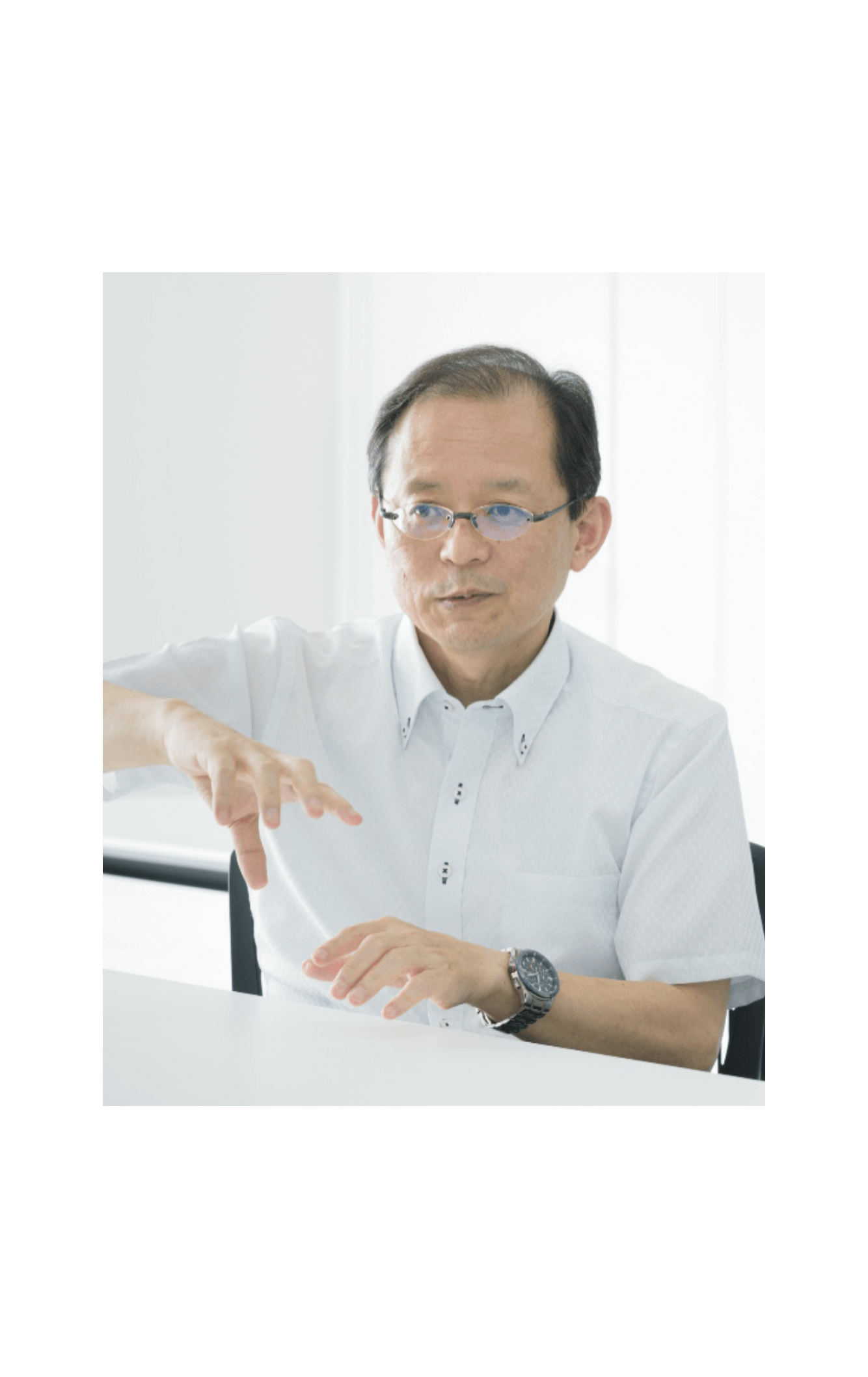
In April 2008, Sony had a great success in developing the back-illuminated CMOS image sensor and was about to launch a camcorder equipped with it, when a seasoned engineer joined the CMOS image sensor development team. This was Taku Umebayashi, who had been working in the area of mass production technology for logic IC for many years.
“As soon as I joined the team, my supervisor came to me and said that they wanted to apply the back-illuminated CMOS image sensor for camcorders to mobile phone cameras.”
The mobile phone cameras of the time were not very developed, and the photos they produced were rather grainy. They were far behind the standard digital cameras in terms of sensitivity, and the images had noticeable levels of noise. It was obvious even then that a wide diffusion of mobile phones would lead to people’s desire to take photos freely in more diverse situations, and that cameras would be expected to offer higher picture quality and more capabilities so that people could enjoy taking photos and movies in a multitude of contexts.
With this in mind, Sony launched a back-illuminated CMOS image sensor for mobile phones in 2010. However, it was evident that the image quality and capability enhancement were far short of the levels expected of future mobile phone cameras. What is more, this product cost more to produce than the existing mobile sensors.
Cameras were already an important criteria for users to choose their mobile phones those days. Mobile phone manufacturers were grappling with the mammoth challenge of developing cameras easy and fun to use and, at the same time, cheaper to make in order to keep handset prices low.
When smartphones came into the scene, cameras were no longer devices simply to capture and save still and moving images. User needs were diversifying and the cameras assumed more purposes—namely, a means to enjoy online contents in combination with various smartphone applications.
As a supplier of camera components, Sony was keenly aware of the need to offer image sensors that were low cost and had enhanced features, capable of supporting continued advancement of the mobile cameras.
The challenge was self-contradictory: to produce an image sensor with higher capabilities and image quality without increasing its size, and what is more, without costing more despite increased manufacturing processes. Moreover, Umebayashi had no previous experience in the image sensor development. What saved him was his expertise in logic IC mass production technology.

Umebayashi first took his familiar course of ideas as a mass production technology engineer and looked into the ways to make smaller sensors at lower cost.
”My immediate idea was to produce more chips from one wafer to reduce the cost.”
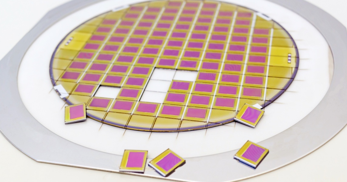
The image sensor chips are formed in multiple numbers on a thin silicon substrate called a wafer. He thought that reducing the surface area of one chip would lead to more chips being formed on a wafer and lower the unit cost of the device.
How can we reduce the chip surface area? This question ultimately led to the idea of “stacking” structure.
“The pixel and circuit sections were normally arranged side by side on the same surface, but I thought of separating them and putting one on top of the other. In this way, a single chip would have a smaller area. I used the rough drawing of an image sensor under development at the time and made a concept drawing to find that the surface area would be reduced almost to a half.”
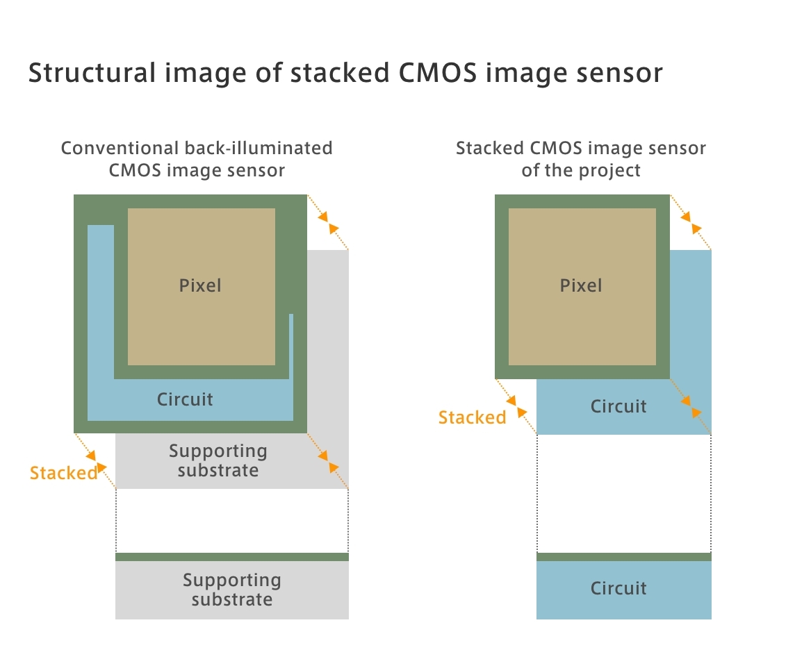
The conventional back-illuminated CMOS image sensor had a layer that bore both the pixel and circuit sections with a “supporting substrate” stuck underneath. The substrate was needed to stabilize the wafer-thin upper layer. Umebayashi’s idea “stacking structure” was to replace the supporting substrate with a circuit chip and laying the pixel chip on top of it. Moving the circuit part to beneath the pixel part would economize the overall surface area of a chip.
If this two-layer structure was realized, the circuit chip would have some room for miniaturization independent of the pixel section, possibly with a large signal processing circuit to realize higher image quality and enhanced capabilities at lower power consumption levels. The structure would offer more than smaller size and lower cost.
Umebayashi prepared a concept design for the stacked CMOS image sensor in about 6 weeks and presented it to his supervisors, who gave him the go-ahead for the project.
The development project for stacked CMOS image sensor was launched in August 2008 with a small team of 5 dedicated members. It was relatively a trouble-free journey up to the concept design, but the real challenge was to translate the design into a physical form. This was the beginning of struggles for the team, eventually lasting for nearly one year and a half.

One of the major obstacles was the process of layering the pixel and circuit wafers together.
“It is imperative to have an absolutely flat surface to layer the chips together. You can imagine it is like sticking a protective sheet on your smartphone screen. It must be completely hermetic, not even a tiniest bubble is allowed.”
This proved to be an insurmountable challenge, for the wafer was very thin and hard. Moreover, if the two chips are even slightly misaligned, the contacts that connect the pixel and circuit will fail and the device will not function as an image sensor.
Analogizing a wafer to a baseball ground, Umebayashi explains that the precision required in this process is like “layering two 120-meter-wide baseball grounds, one on top of the other, with less than 1 mm of margin of error.” In actual terms, the margin is within 2.5 μm. If unsuccessful, the product does not produce any image. This meant a super-tricky maneuver that would make even the most experienced engineers in semiconductor manufacturing struggle.
Facing the formidable hurdle to overcome, Umebayashi and the team took a very simple approach. They faithfully followed a PDCA cycle: each member came up with an idea how best to layer the wafers together, test the idea, review the results, then plan for further experimentation. Because they started as a small team, human and financial resources were not abundantly allocated to the project. The team was repeating the cycle persistently, and after some time, they gained allies outside the team, including a circuit design engineer who joined the efforts and a process design engineer who tried every possibility with unyielding determination. Eventually, the project seemed to be heading to a bright outcome.
However, the tide was suddenly turned. The management was very keen to see further progress and requested the team to “establish the stacking technology by the end of the year (2009)” because they wanted to “carry out an image output test on a pilot line, starting from spring 2010.” This development put Umebayashi and the team before an imminent deadline.
This was an unexpected wake-up call. They accelerated their efforts, but the end-of-the-year deadline could not be met. Umebayashi had to negotiate with the supervisor, saying “we will make it by the beginning of next year.” The mood was that they could not possibly ask to push the deadline further back.
By this time, more than one year had elapsed since the project was launched to develop the stacked CMOS image sensor. Many colleagues in the company had no idea what the team was up to. Umebayashi recalls that it was not an easy time.
“At home, I was acting as if everything was fine, but deep down, I was panicking as I lived through that year-end period. It crossed my mind that, if we failed to find a solution and the pilot in spring ended in a shambles, perhaps I have no option but to hand in my notice. I was under an enormous stress.”


“Somehow the trial went well, Umebayashi-san!”
In the new year, they managed to succeed in layering to the extent that it stood a flow production of prototypes. Still, the production was a precarious affair, checking the wafer conditions each time. Every moment was critical. In the end, the flow production was sustained till the last prototype, and some good chips came out of it, showing signs of electrical conductivity between the upper and lower chips, despite the pitiful yields. The pilot scheduled in March 2010 thus ended more or less successfully, though the image output was only in black and white. However, Umebayashi was convinced, based on the proof of electrical conductivity, that the stacking structure could be technically achieved.
Sony started moving toward commercialization of the image sensor in full throttle at the same time as Umebayashi and the team pressed on to verify the image output in color. The Kumamoto Technology Center embarked on prototyping for mass production. When a sample was made and put to an internal pilot, everyone present was stunned by the output image and the small size of the chip: the quality and brightness of the image was no less than that of the back-illuminated CMOS image sensor of the time.
“They looked at the stacked chip through a microscope astonished and said, ‘Wow, how does it work, such a tiny chip only with some pixels?’ They could not see the circuit chip because it was hidden behind the pixel chip.”
Already 3 years and 9 months passed since Umebayashi joined the stacked sensor project team. Finally, Sony announced the development of its stacked CMOS image sensor in January 2012, and the shipment started in October, following the product launch in August of the same year.
“I saw an article about the tablet device by some manufacturer that was the first to implement our image sensor. The title ran, ‘Adopting the stacked CMOS image sensor.’ I was over the moon and immediately saved the article.”
Later, the stacked CMOS image sensor became a talking point when it was introduced in the Xperia Z SO-02E, a smartphone by Sony Mobile Communications (renamed Sony) which offered superior imagery capabilities, including the HDR (high dynamic range) video capture that made vibrant movies possible even in high-contrast settings. Its reputation was catalytic to the growing number of manufacturers that sought after Sony’s stacked CMOS image sensors.
“I believe that our competitors were taken aback when Sony announced the stacked sensor because the development had been kept secret. What’s more, they could not copy us so easily. In fact, it took them two years to produce their versions of stacking technology. I bet they had a terrible time trying to stack wafers together. ”
According to a US research firm, Strategy Analytics, the market for CMOS image sensors for mobile applications in 2021 grew 3% year on year to 15.1 billion dollars, and Sony Semiconductor Solutions has the largest share, accounting for 45%.
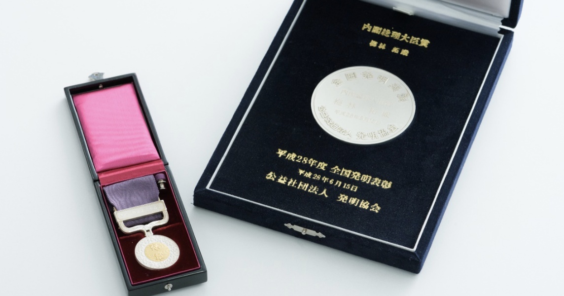
In April 2021, Umebayashi was decorated with the Medal with Purple Ribbon, an honorable recognition accorded to individuals who made outstanding contributions in academia, sports or arts, such as inventions and discoveries in science and technology. He received one for the stacked CMOS image sensor as its diffusion through smartphones and other diverse products delivered more convenience to people’s lives and, also, stimulated the semiconductor industry in Japan.
“In hindsight, there was always something that helped me, like a lucky breakthrough or someone offering a helping hand. There were a few miraculous occasions, and also the support of so many people. I was so lucky.”
Umebayashi looks back the project days emotionally.
Sony’s image sensor engineers always aspired to pioneer for a new world and their diligent efforts bore fruit through the generations of CCD, back-illuminated CMOS, and stacked CMOS image sensors.
The journey is not over yet. Our engineers with inexorable ambitions continue to aim for better image sensors.
