Semiconductor project launched by Sony.
History of Sony's Semiconductors - Timeline
It introduces the history of Sony's semiconductor business, which began in 1954 with the commercialization of transistors for the first time in Japan.
- Home
- Group Information
- History of Sony's Semiconductors - Timeline
| History of Sony's Semiconductor | History of SSS Group's sites | |
|---|---|---|
|
|
||
|
Successfully prototypedJapan's first transistor. 
|
||
|
Invented the tunnel (Esaki) diode. 
|
||
|
Developed silicon power transistors. 
|
||
|
1960 |
Atsugi plant construction completed by Sony. 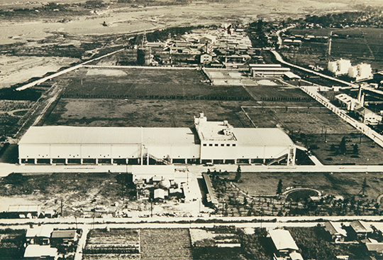
|

|
|
Commercialized the world'sfirst monolithic IC for small radios. 
|
||
|
Developed the Sony Magnetodiode (SMD), a new semiconductor device. 
|
||
|
Sony Shiroishi Semiconductor established. 
|
||
|
1970 |
Development of CCD image sensors begins. |
|
|
Succeeded in 8x8 pixels imaging 
|
||
|
Sony Kokubu Semiconductor established. 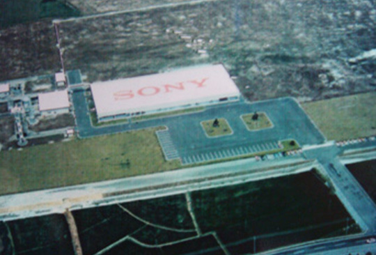
|
||
|
Mass production begins on variable capacitance diodes (varicaps) for electronic UHF/VHF tuners. Commercialized highly reliable MNOS nonvolatile memory for TV tuners. |
||
|
Developed a 110,000-pixel CCD imager. 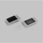
|
||
|
1980 |
Commercialized the first CCD image sensor.CCD color camera "XC1" adopted by jumbo jet. 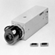
Developed the MCZ method of silicon crystal growth. 
|
|
|
Developed LSI circuits enabling production of consumer CD players. 
|
||
|
Commercialized two models of laser diodes produced using MOCVD, a world first. 
|
Sony Oita established. 
|
|
|
Developed LSIs for digital audio tape recorders(DAT). |
Sony Technical Soft established. 
|
|
|
Commercialized the world's first ultra-high-power laser with optical power output of 1 W. 
|
Sony Nagasaki established. |
|
|
Commercialized a 1/2-inch, 250,000-pixel CCD image sensor for passport-sized Handycam. 
Successfully developed the world's first high-speed 4 Mb SRAM. 
|
||
|
1990 Company name changed from Sony Technical Soft to Sony LSI Design. |
Developed the world's first 1-inch, 2-megapixel FIT CCD sensor for HDTVs. 
|
|
|
Sony Kokubu Semiconductor renamed Sony Kokubu. Sony LSI Design Head office relocated to YBP East Town, 11F (until 2012). |
||
|
Developed a MUSE decoder LSI for HD broadcasts. 
Developed a 2/3-inch, 2-megapixel FIT CCD sensor for HDTVs. 
Commercialized a dedicated LSI for MiniDisc system. 
|
||
|
Developed the world's fastest 16 Mb SRAM. 
Commercialized the world's smallest color TFT LCD (0.55 inches, 113,000 dots) and a 0.7-inch color LCD with the world's highest pixel count (180,000 dots). 
|
||
|
Commercialized a 1/4-inch, 410,000-pixel color CCD image sensor. 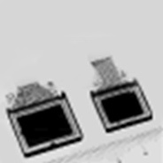
|
||
|
Commercialized an LSI conforming to the IEEE 1394 high-speed serial bus specification. 
|
Sony LSI Design Head office relocated, Atsugi operations integrated (YBP research building). 
|
|
|
Established a low-temperature polysilicon TFT molding technique. 
Commercialized an LSI with embedded DRAM for MiniDisc applications. 
Development of CMOS Image Sensors begins. |
||
|
Developed a single-chip MPEG-2 video encoder LSI. 
Developed a 2.5-inch, 180,000-dot low-temperature polysilicon TFT LCD and a 1/3-inch, 680,000-pixel CCD (340,000 effective pixels). 

|
||
|
Commercialized the EXview HAD CCD, with high-sensitivity sensing also in the near-infrared spectrum. |
||
|
Developed a single-chip, two-wavelength laser diode for CD recording/playback and DVD playback. |
||
|
2000 Commercialized the first CMOS image sensor "IMX001". Incorporated into AIBO. |
Sony LSI Design Kyushu Branch opened. (Later designated as head office.) 
|
|
|
Developed two system LSIs with low power consumption for Network Handycam. Developed a high-temperature polysilicon TFT LCD panel (0.9-inch XGA, aperture ratio: 66.1%) using an ultra-wide-aperture process. 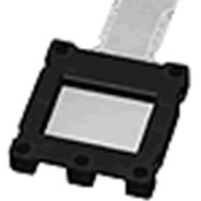
|
Three Kyushu sites (Sony Kokubu, Sony Oita, and Sony Nagasaki) integrated; Sony Semiconductor Kyushu established. Sites renamed Kokubu Technology Center , Oita Technology Center , and Nagasaki Technology Center, respectively. Sony Semiconductor Kyushu Kumamoto Technology Center established. 
|
|
|
Commercialized an ultra-small TV tuner module 1.5 ml in volume. 
Developed Virtual Mobile Engine reconfigurable circuit technology. 
|
Sony LSI Design Atsugi office opened. |
|
|
Developed the world's first monolithic high-output two-wavelength laser diode. 
Developed the world's first single-chip LSI for GPS applications. 
Developed a four-color filter CCD that halves color reproduction errors, as well as a supporting image processor. 
Commercialized a 220 mW laser diode (highest level of output in the industry) enabling 16× DVD recording. |
||
|
Commercialized the first consumer 1080i-compatible HD CCD, supporting high-definition 1080i recording at a 16:9 aspect ratio. 
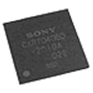
Developed a single-chip MPEG codec LSI (CXD4702GB) for high-quality recording/playback. 
Decision making of shifting focus from CCD to CMOS image sensors. |
Sony Computer Entertainment fab integrated (incorporated into Nagasaki Technology Center). |
|
|
Commercialized the first CMOS sensor (1/3-inch type, 2.97 megapixels) for consumer HD digital video cameras. 
Commercialized a new SXRD: world's smallest (0.61-inch type) full HD reflective liquid crystal display device. 
Commercialized a compact digital tuner module enabling 1 seg digital terrestrial TV broadcast reception on mobile devices. 
|
||
|
Commercialized ClearVid CMOS sensors with a new structure enabling both high resolution and high sensitivity. 
Commercialized a 10.2-megapixel APS-C CCD image sensor for consumer digital still cameras. 
Cell Broadband Engine&trade mass production begins. 
|
Sony Semiconductor Kyushu Kokubu Technology Center renamed Kagoshima Technology Center. |
|
|
Commercialized BrightEra 0.79-inch type transmissive microdisplays employing inorganic alignment film, with the world's highest brightness. 
Commercialized a high-power blue-violet laser diode for Blu-ray discs compatible with dual layer, 2×–4× recording. 
Commercialized an APS-C size CMOS image sensor for DSLRs offering an industry-leading resolution of 12.47 effective megapixels. 
Developed a 0.61-inch type full HD SXRD for projectors that supports high frame rates. 
|
||
|
Developed a 35mm full-frame CMOS image sensor for DSLRs offering a resolution of 24.81 effective megapixels and high-speed readout. 
Developed a back-illuminated CMOS image sensor with high image quality from low noise and nearly double the sensitivity of conventional sensors. 
Commercialized a CMOS image sensor for mobile phones with the industry's highest resolution of 12.25 effective megapixels, a world first. 
|
Nagasaki Semiconductor Manufacturing Corporation jointly established by Toshiba Corporation, Sony Corporation and Sony Computer Entertainment Inc.(Current : Sony Interactive Entertainment Inc.). |
|
|
Commercialized World’s first back-illuminated CMOS image sensor. Installed into 2 digital high vision Handycams. Commercialized the world's first TransferJet-compatible LSIs. 
Commercialized the world's first demodulator LSI for DVB-T2 digital terrestrial broadcasts. 
|
||
|
2010 |
Launched the industry's first high-power (400 mW class) blue-violet laser diode for BDXL™-compatible Blu-ray discs. 
Commercialized a back-illuminated CMOS image sensor for mobile phones with a resolution of 16.41 effective megapixels, a world first. 
Newly developed Super 35 mm-equivalent CMOS image sensor for digital cinema camcorder. 
|
|
|
Newly developed SXRD: world's smallest (0.74-inch type) 4K reflective liquid crystal display device. 
|
Sony Shiroishi Semiconductor absorbed into Sony Semiconductor Kyushu. Company name changed to Sony Semiconductor. Sony Shiroishi Semiconductor renamed Shiroishi-Zao Technology Center. |
|
|
Developed next-generation Crystal LED Display technology, ideally suited to large screens and high picture quality. Developed stacked CMOS image sensors, which have enabled the ongoing evolution of cameras. These models introduced RGBW coding and HDR movie functions. Developed next-generation back-illuminated CMOS image sensors, again supporting ongoing evolution of cameras. Jointly developed low-power LSIs for wideband millimeter-wave wireless communication offering the world's fastest transfer rate of 6.3 Gb/s. Developed the world's first true-green laser diode with optical power output surpassing 100 mW at a wavelength of 530 nm. 
|
Sony LSI Design Kyushu head office renamed as Fukuoka Branch. Higashiura Satellite established in the Higashiura Plant of Japan Display West in Chita, Aichi. Took over laminate substrate production of Sony Chemical & Information Device after this business was split off. Neagari Site established. |
|
|
Commercialized mobile device global navigation satellite system (GNSS) receiver LSIs with the industry's lowest power consumption of 10 mW. 
|
Head office relocated to Kikuchi-gun, Kikuyo-machi, Kumamoto Prefecture. |
|
|
Start of external sales of highly durable and heat-resistant SoRPlas™ flame-retardant recycled plastic with up to 99% recycled content. Commercialized the world's highest-sensitivity CMOS image sensor for automotive cameras. 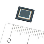
Commercialized the industry's first stacked CMOS image sensor with an image plane phase detection signal processing function for high-speed AF. 
|
Neagari Site closed due to termination of laminate substrate business. Acquired the Tsuruoka Factory of Renesas Yamagata Semiconductor Co., Ltd., a wholly-owned subsidiary of Renesas Electronics Corporation, Sony Semiconductor Corporation's Yamagata Technology Center was established. 
Sony LSI Design Head office relocated (Atsugi). 
|
|
|
World’s first Cu-Cu (Copper-Copper) connection technology enters mass production. |
Acquired Softkinetic Systems S.A., a Belgian company specializing in ToF sensor technology. |
|
|
Commercialized the industry's first stacked CMOS image sensor with built-in hybrid autofocus and 3-axis electronic image stabilization. 
Commercialized the industry's first ISDB-S3 compatible demodulator LSI and tuner modules for 4K/8K digital satellite broadcasts. 

|
Acquired Altair Semiconductor, an Israeli company specializing in LTE modem chip technology. Sony semiconductor business spun off from Sony Corporation as a subsidiary, starting business as Sony Semiconductor Solutions. 
Company name changed to Sony Semiconductor Manufacturing. Oita Technology Center established in the city of Oita. Plant in Kunisaki renamed as Oita Technology Center Kunisaki Satellite. 
|
|
|
Developed the industry's first 3-layer stacked CMOS image sensor with DRAM for smartphones. Commercialized the industry's first CMOS image sensor for automotive cameras that both mitigates LED flicker and enables HDR shooting. 
Developed original low-power wide-area (LPWA) network technology. Commercialized a high-speed vision sensor enabling object detection and tracking at 1,000 fps. 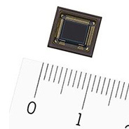
Developed a back-illuminated ToF image sensor with the industry's smallest pixel size. Commercialized the industry's highest resolution 7.42 effective megapixel stacked CMOS image sensor for automotive cameras. 
Commercialized a back-illuminated ToF sensor. 
|
||
|
Commercialized SPRESENSE™, a low-power board equipped with a smart-sensing processor for IoT applications. 
Commercialized a 0.5- type OLED microdisplay withtop-of-class UXGA resolution. 
Commercialized a new SXRD™: the world's smallest (0.37-type) full HD reflective liquid crystal display device, and a dedicated signal processing drive LSI. 
Commercialized a stacked CMOS image sensor for smartphones with the industry's highest 48 effective megapixels. 
Commercialized a CMOS image sensor for automotive cameras that mitigates LED flicker and enables HDR shooting with the industry's highest 5.4 effective megapixels. 
|
||
|
Commercialized a communication module compatible with proprietary ELTRES™ low-power wide area (LPWA) wireless communication standard. 
Commercialized two types of 4K-Resolution CMOS image sensors for security Cameras: world's Smallest type 1/2.8 and enhanced low-light performance type. 
Commercialized six types of stacked CMOS image sensors with global shutter function with back-illuminated pixel structure. 
|
Acquired Mido Holdings, a network virtualization technology developer. |
|
|
2020 Sony Semiconductor Solutions' Osaka Office opened. Company name changed from Altair Semiconductor to Sony Semiconductor Israel. Sony Semiconductor Energy Management established. |
Newly developed stacked event-based vision sensor with the industry's smallest pixels and highest HDR performance by Sony and Prophesee Commercialized two models of SWIR image sensors for industrial equipment capable of capturing images across both the visible and invisible light spectrums, with the industry’s smallest 5μm pixel size 
Commercialized two models of world’s first intelligent vision sensors with AI processing functionality 
Commercialized high-precision GNSS receiver LSIs for IoT and wearable devices delivering the industry’s lowest power consumption for dual-band positioning operation 
|
|
|
Commercialized Large Format CMOS Image Sensor with Global Shutter Function and Industry’s Highest Effective Pixel Count of 127.68 Megapixels 
Commercialized 1/1.2-type 4K-Resolution CMOS Image Sensor for Security Cameras with Approximately 8 times the Dynamic Range of Conventional Model in a Single Exposure 
Commercialized a Stacked SPAD Depth Sensor for Automotive LiDAR Applications, an Industry First 
Commercialized Two Types of Stacked Event-Based Vision Sensors with the Industry’s Smallest 4.86μm Pixel Size for Detecting Subject Changes Only 
Commercialized UV Wavelength-Compatible CMOS Image Sensor Equipped with Global Shutter Function and Industry’s Highest Effective Pixel Count of Approx. 8.13 Megapixels 
Launched Edge AI Platform Service AITRIOS™ Newly Developed World’s First Stacked CMOS Image Sensor Technology with 2-Layer Transistor Pixel |
||
|
Launched Fee-Based Service on Edge AI Sensing Platform AITRIOS™ |
Sony LSI Design absorbed into Sony Semiconductor Solutions for business integration |
|
|
Commercialized SPAD Depth Sensor for Smartphones with High-Accuracy, Low-Power Distance Measurement Performance, Powered by the Industry’s Highest Photon Detection Efficiency 
|
||


Contact Us
For inquiries about Sony Semiconductor Solutions Group and products / solutions, specifications, quotation / purchase requests, etc., please contact us using the Inquiry form from the button below.