
SPAD ToF Depth Sensor
1/2.9" 0.1MP IMX560
Compact yet achieves high resolution
Overview
Time of Flight (ToF) depth sensors measure the distance to a target object by emitting light from a source, usually a laser or LED, and detecting the reflected light, based on the time elapsed between the two. Its single photon avalanche diode (SPAD) pixels have a structure that uses "avalanche multiplication" to amplify electrons from a single incident photon, causing a cascade like an avalanche. This enables the sensor to detect even low levels of light. Using SPAD light-receiving pixels, the sensor detects flight time of light, achieving long-range and high-accuracy distance measurement.
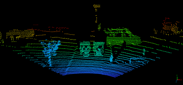
As high-accuracy compact sensors that can capture range information across a wide area including long distances, SPAD ToF depth sensors are suited to detecting people and objects, including automated guided vehicles (AGVs) and autonomous mobile robots (AMRs). Their resistance to noise raises expectations for use in outdoor applications such as smart infrastructure and 3D mapping.
Features
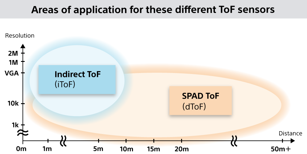
Capable of long-range 3D sensing
SPAD ToF depth sensors have a mechanism of avalanche-multiplying electrons when photons hit, and amplifies the photons detected for conversion to powerful signals. This allows faint light signals returning over long distances to be detected with high accuracy. Sensors of this type can measure more than a few dozen meters ahead and are capable of grasping 3D conditions in a wider area than the indirect ToF (iToF) sensor type. It can be used to detect objects in a wide area, such as AGVs and AMRs that autonomously travel while sensing for obstacles ahead, and for safety light curtains which protect people moving around in a specific area by identifying in advance any risk of entry.
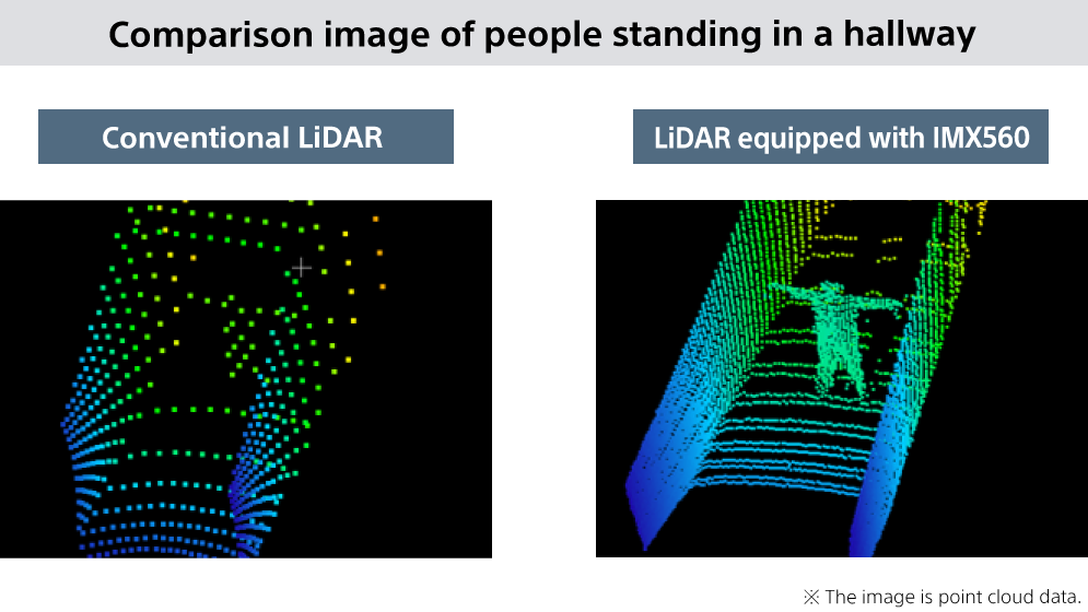
High resolution
SPAD ToF depth sensors are equipped with on-chip time-to-digital converters (TDCs) and are capable of digital output. By implementing a layered design and arranging many TDCs in parallel, Sony has achieved high resolution with the capability to measure multiple points simultaneously. This improves object recognition accuracy.
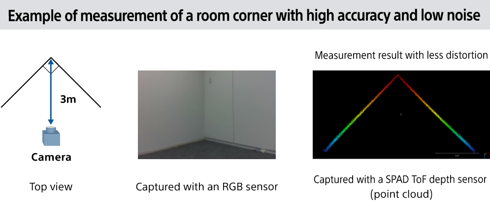
Depth sensing system resistant to multi-path interference
For accurate distance measurement, it is important to remove signals reflected in unintended paths against the signal emitted from the camera's light source and reflected on the target just once before reaching the sensor. In particular, concave shapes such as the corner of a room tend to cause signal light in unintended paths, which may result in erroneously measured values. The depth sensing algorithm of the SPAD ToF depth sensor measures the distance to the object several times and statistically processes the measurement results of each point acquired. This allows high-accuracy and low-noise data to be stably acquired and provides the capability of distortion-free measurement, even of corners. This leads to improved reliability of measurement and expectations for ensured accuracy in various applications.
Compact and designed for easy system integration
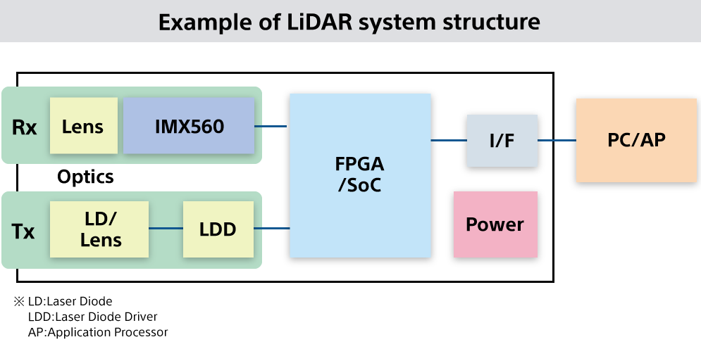
Sony’s proprietary pixel technologies nurtured in CMOS image sensor development have been used to incorporate SPAD pixels and a depth-sensing processing circuit into a single chip. This achieves high resolution with a compact size, and allows the LiDAR structure to be simplified. This is ideal for applications requiring low power consumption, compactness, and adaptability. By integrating these capabilities into a single chip, it also helps lower the cost of LiDAR.
Technology
Sony’s SPAD ToF depth sensors integrate a pixel chip (top) using back-illuminated SPAD pixels and a logic chip (bottom) equipped with distance-measuring processing circuits, stacked with Cu-Cu connection, ensuring each pixel is connected. By placing the circuit section beneath the pixel section, it secures the aperture ratio※ while achieving a fine pixel size of 10 μm square as a SPAD depth sensor. In addition, the following innovations are applied to pixels.
・A textured surface is applied to the light entry point to diffract incoming light, significantly enhancing absorption.
・Optimizing the design of the avalanche region within each pixel enables more efficient generation of the multiplication effect.
These proprietary pixel structures enable detection with high resolution and distance resolution even of distant objects with low reflectivity. Furthermore, the stacked structure with Cu-Cu connection for each pixel enhances the readout speed. The capability of high-accuracy, high-speed distance measuring from long to short ranges helps to improve detection and recognition performance and reduces power consumption of the entire system.
* The ratio of the aperture area (excluding the light-shielding area) is seen from the light incident surface side per pixel. The wider the aperture area, the higher the detection efficiency.
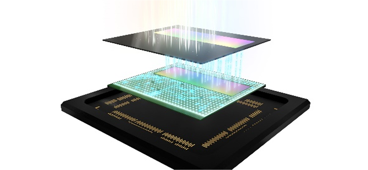
(Top: SPAD pixels, bottom: distance measuring processing circuit)
In addition, the unique signal processing function is integrated into the sensor’s logic chip. This enables the sensor to cover the process of converting raw data acquired from SPAD pixels into range data to be output. This capability reduces the burden of post-processing, allowing simplified development of the entire system.
Find out more about the ToF technology.
Specifications
| Model Name | IMX560-AAMV |
|---|---|
| Pixel | SPAD (Single Photon Avalanche Diode) pixel |
| Image size | Diagonal 6.25 mm (Type 1/2.9) |
| Number of effective pixels | 597 (H) × 168 (V) approx. 100K SPAD pixels |
| Unit cell size | 10.08 µm (H) × 10.08 µm (V) |
| Element size | 3 (H) × 3 (V) SPAD pixels ( i.e. 199 (H) x 56 (V) elements) |
| Frame rate (Max.) | 100 frame/s*1 |
| Recommended light source wavelength | 850 nm, 905 nm, 940 nm etc. |
| Photon detection efficiency | 24% (905 nm) |
| Sampling frequency | 1 GHz / 0.5 GHz |
| Output interface | MIPI CSI-2 (4 lane / 2 lane) |
| Readout mode | Line mode / Array mode*2 |
| Package | 152-pin BGA 15.35 mm (H) × 15.65 mm (V) |
| Product overview PDF |
 IMX560-AAMV
|
* Values are subject to change without prior notice.
*1 The frame rate trades off with the number of samplings.
Increasing the number of samplings improves accuracy but decreases the maximum frame rate.
*2 Array mode: 1D-addressable (rolling).
Applications
Find out more about SPAD ToF depth sensor applications.
Download
IMX560-AAMV Product Overview
This document summarizes the product overview, features, and specifications.
A List of Cameras with ToF Image Sensors
You can download a list of cameras with Sony's ToF image sensors here.
Related Products & Solutions
-
Image Sensor
iToF Image Sensor IMX556/IMX570
High-speed, high-resolution iToF image sensor that excels at near- to mid-range sensing
-
Image Sensor
Time of Flight Image Sensor (Overview)
See here for the ToF image sensor overview page
Product & Service Inquiries
Click here to request for a datasheet/quotation (RFQ)!
* This button will redirect you to the salesforce.com Co., Ltd. website,
which we have entrusted.
E-mail Newsletters
Find the latest information on our newsletter for industrial and security applications.