Atsugi, Japan — Sony Semiconductor Solutions Corporation (SSS) today announced the upcoming release of the IMX900, a 1/3-type-lens-compatible, 3.2-effective-megapixel*1 stacked CMOS image sensor with a global shutter for industrial use that boasts the highest resolution*2 in its class.
The new sensor product employs an original pixel structure to dramatically improve light condensing efficiency and near infrared sensitivity compared to conventional products, enabling miniaturization of pixels while maintaining the key characteristics required of industrial image sensors. This design achieves the industry’s highest resolution*2 of 3.2 effective megapixels for a 1/3.1-type, global shutter system which fits in the S-mount (M12), the mount widely used in compact industrial cameras and built-in vision cameras.
The new product will contribute to the streamlining of industrial tasks in numerous ways, by serving in applications such as code reading in the logistics market and assisting in automating manufacturing processes using picking robot applications on production lines, thereby helping to resolve issues in industrial applications.
*1 Based on the image sensor effective pixel specification method.
*2 Among CMOS image sensors with a global shutter that are compatible with 1/3-type lenses for industrial use. As of announcement on October 13, 2023.
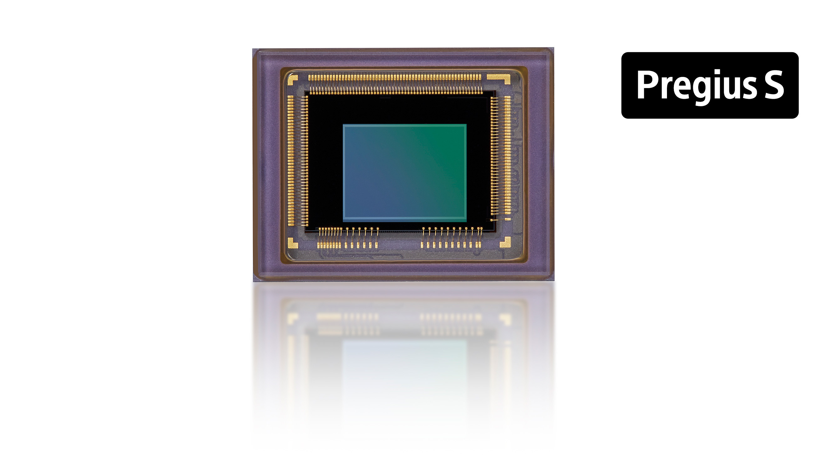
CMOS image sensor IMX900
| Model name | Sample shipment date (planned) |
|---|---|
|
IMX900 1/3.1-type (5.81 mm diagonal) 3.2-effective-megapixel*1 |
October 2023 |
With demand for automation and manpower savings on the rise in every industry, SSS’s original Pregius S™ global shutter technology contributes to improved image recognition by enabling high-speed, high-precision, motion distortion-free imaging in a compact design. The new sensor utilizes a unique pixel structure developed based on Pregius S, moving the memory unit*3 that was previously located on the same substrate as the photodiode to a separate signal processing circuit area. This new design makes it possible to enlarge the photodiode area, enabling pixel miniaturization (2.25 μm) while maintaining a high saturation signal volume, successfully delivering a higher pixel count of approximately 3.2 effective megapixels for a 1/3.1-type sensor.
Moving the memory unit to the signal processing circuit area has also increased the aperture ratio, bringing significant improvements to both incident light angle dependency*4 and quantum efficiency. These features enable a much greater level of flexibility in the lens design for the cameras which employ this sensor. Additionally, a thicker photodiode area enhances the near infrared wavelength (850 nm) sensitivity, and nearly doubles the quantum efficiency compared to conventional products.*5
This compact, 1/3.1-type product is available in a package size that fits in the S-mount (M12), the versatile mount type used in industrial applications. It can be used in a wide range of applications where more compact, higher performance product designs are desired, such as in compact cameras for barcode readers in the logistics market, picking robot cameras on production lines, and the automated guided vehicles (AGVs) and autonomous mobile robots (AMRs) that handle transportation tasks for workers.
*3 Memory that temporarily stores signals.
*4 Light condensing characteristics for light incidence on the pixels of an image sensor at an angle.
*5 Compared with SSS’s 1/2.9-type, 1.58-megapixel IMX296 CMOS image sensor.

Cross-section of pixel structure
Product using conventional Pregius S technology (left) and the IMX900 using the new pixel structure (right)
Main Features
- Industry’s highest resolution*2 for an image sensor with a global shutter compatible with a 1/3-type lens, at approximately 3.2 effective megapixels
- Vastly improved incident light angle dependency lend greater flexibility to lens design
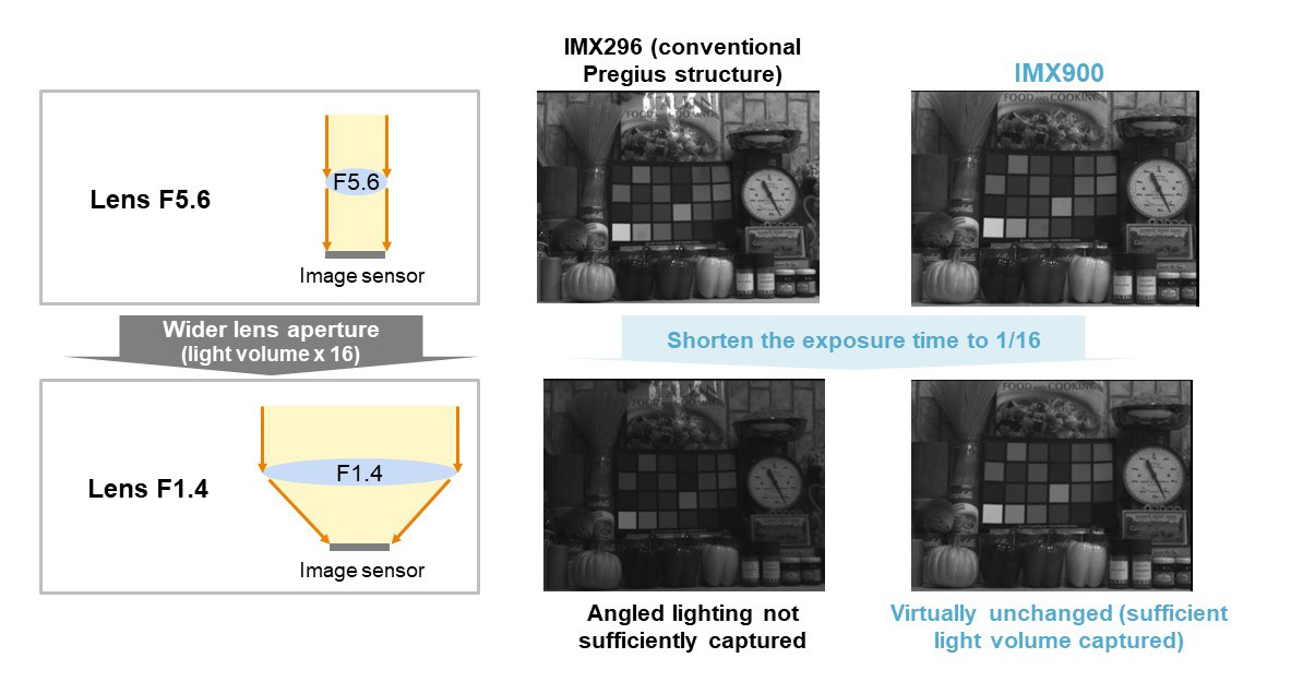
Example of effects due to improved incident light angle dependency
- Delivers approximately double the quantum performance of conventional products*5 in the near infrared wavelength
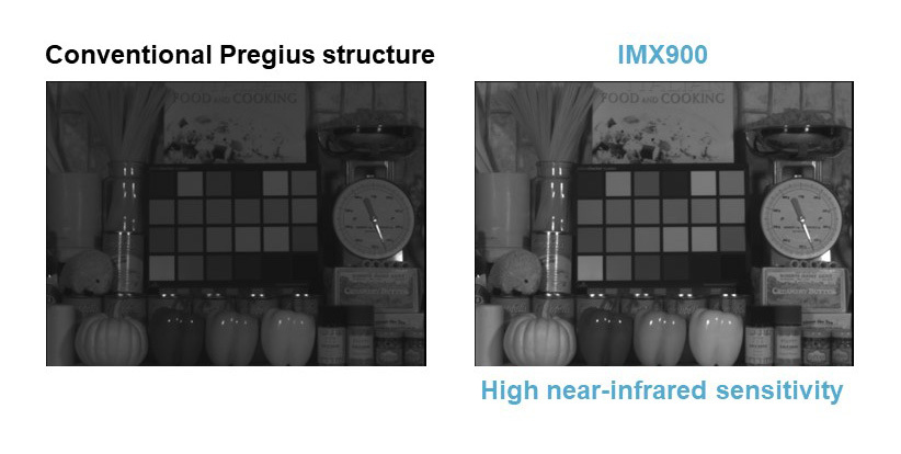
Imaging comparison using near-infrared lighting (850 nm)
(Comparison in 2.25 μm pixel equivalent using conventional Pregius structure)
- Includes on-chip features for greater convenience in reducing post-production image processing load
Various features are included on this product to lighten the post-production image processing load and improve recognition precision, such as Fast Auto Exposure, which enables high-speed calculation and configuration of optimal exposure times, and Quad HDR, which expands the dynamic range by setting multiple exposure times in units of four pixels each. These features help streamline camera design, reduce cost, and improve recognition precision.
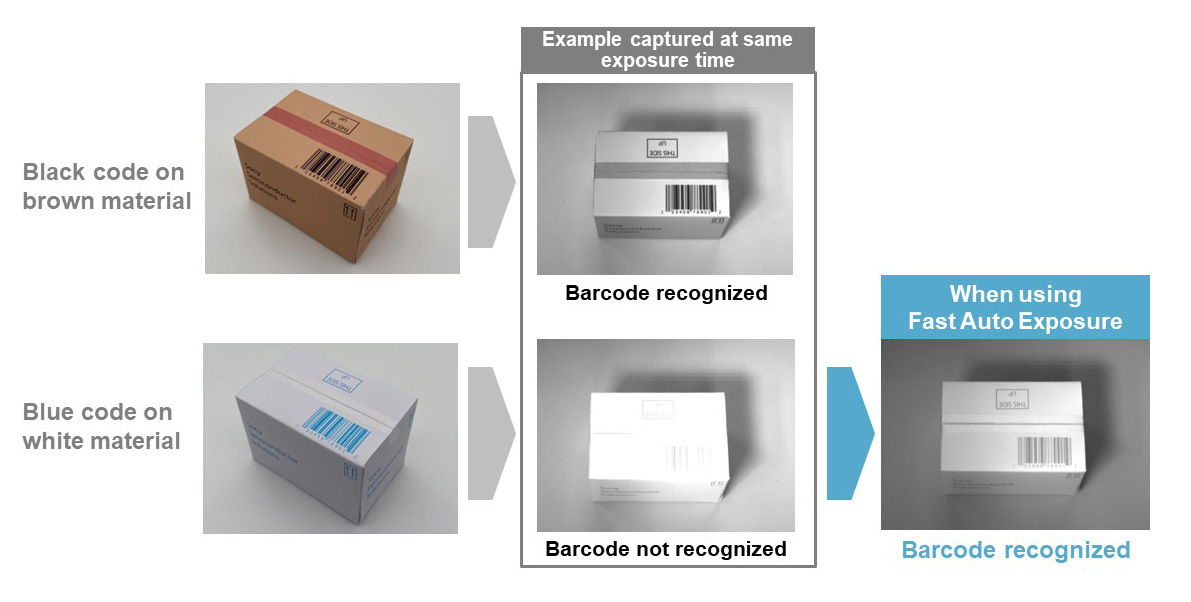
Usage example of Fast Auto Exposure function
- High-speed, 113 fps*6 imaging
*6 At 10-bit output.
Please visit the following websites for more information.
-IMX900 product information:
https://www.sony-semicon.com/en/products/is/industry/gs/imx900.html
-Global shutter technology:
https://www.sony-semicon.com/en/technology/industry/pregius.html
| Model name | IMX900 | ||
|---|---|---|---|
| Effective pixels |
Approx. 3.2 megapixels |
||
| Image size |
Diagonal 5.81 mm (1/3.1-type) |
||
| Unit cell size | 2.25 μm × 2.25 μm | ||
| Frame rate | All pixels |
8 bit 120 fps |
|
| Power supply | Analog |
|
|
| Digital |
|
||
| Interface |
|
||
| Main new functions |
Fast Auto Exposure |
||
| Output |
MIPI 4 lane |
||
| Color filter | Bayer/monochrome | ||
| Package |
Ceramic package (LGA) |
||
Pregius / Pregius S, and their logos are the registered trademarks or trademarks of Sony Group Corporation or its affiliated companies.