Striving toward the realization of ultimate digital mirrorless interchangeable-lens cameras
―Tireless attitude is the secret of successful value creation
December 12, 2022
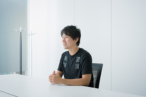
Digital mirrorless interchangeable-lens cameras are entering the mainstream popularity with people who enjoy using them for travels, leisure activities and many other occasions. When it comes to a professional use, however, these devices face demanding expectations for resolution, speed and other performance, even higher than those of the analogue SLR cameras. Sony’s α1 is a flagship model of the full-size mirrorless interchangeable-lens α™ (Alpha™) series camera, which enjoys high professional appraisals for its unmatched resolution and speed, but it is not widely known that it has groundbreaking new technology inside. The back-illuminated stacked CMOS image sensor which has been developed specifically for this model has approximately 50.1 effective megapixels with the 14-bit 250 fps capability. What is more, it has solved the blackout issue that the EVF (electronic view finder) temporarily loses its backlight at every photo shoot. Because of this blackout phenomenon, professional photographers have long adopted a shooting style to keep one eye on the view finder while following the target with the other to ensure that the object stays in the center of the view frame during the blackouts. The blackout-free performance allows the photographer to keep following their target without taking their eyes off the EVF, making sure their desired frame composition. This game-changing new technology was developed by Chihiro Okada of Sony Semiconductor Solutions (SSS), who is an engineer working on the research and development of image sensors. We interviewed him to learn about his approach to developing new technology.
Okada Chihiro
Sony Semiconductor Solutions Corporation
Research Division 1
Profile:Joined Sony Corporation in 2006, Okada worked with a team to develop digital still cameras, where he was responsible for planning specifications of image quality and developing signal processing. He moved to Sony Semiconductor Solutions Corporation in 2011 and started working on analog circuit designs for image sensors. His involvement in the development of ΔΣ ADC to be implemented in α1 cameras started in 2015, and later he assumed a responsibility as a design section leader, overseeing its system designs. He then took up a position in the Research Division 1 in 2019, and currently develops the next-generation depth sensor.
“Do we really need an image sensor which offers nothing more than high speed performance?” A desire to create something of genuine value
Digital cameras normally take two images with one image sensor, one for the photograph and the other for the EVF. While you are following the target, the CMOS image sensor continually reads out images to the EVF, and when you operate the shutter, the sensor switches to the drive mode for capturing a still image. The switching is necessary because of a significant difference in the resolution required for the EVF display and still images. A blackout happens at this point, and it has been structurally unavoidable. Professional photographers were also unsatisfied with the somewhat choppy motion of the target viewed through the EVF, especially with older model cameras, because of the low frame rate of 60 fps. α1’s groundbreaking new architecture realizes both smooth EVF images and blackout-free operation.

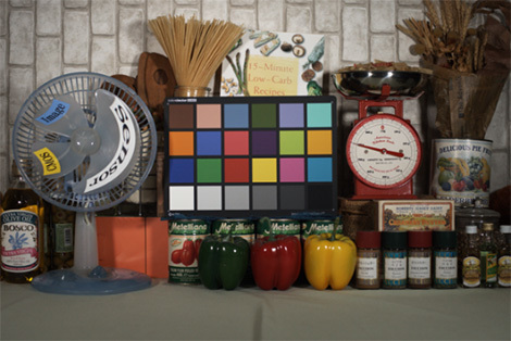
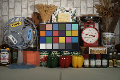
Blackout-free shooting
拡大

One might ask if it was absolutely impossible for a standard digital mirrorless camera to achieve the blackout-free shooting. The answer is no. It is possible if the camera’s EVF is run on two different modes to minimize the time lag of the switching. With two streams of images at different readout speeds, it is possible to fill the gap created by the blackouts by switching to the images from the slower readout. In this case, however, the two streams of images for the EVF are read out at different speeds. In order to compensate the time lag between them, it is necessary to run the faster stream at double the frame rate (for example, if the EVF is to display images at 60 fps, the sensor must capture images at 120 fps). This is because the frames that are out of alignment at the seams are discarded, resulting in the valid frame rate being cut down to a half. To double the speed means, naturally, twice the power consumption. This poses a critical problem considering that the digital interchangeable lens mirrorless cameras are often designed for outdoor use. What is more, α1 was required to implement a 120fps EVF to deliver further enhanced photography experience. This meant that the image sensor needed to realize 240 fps. Therefore, it was urgent to develop a system that allowed high speed readouts at the frame rate of 120 fps for EVF display without increasing the power consumption. The task of overcoming this challenge fell upon Okada.
He saw no particular technical difficulties in achieving the 120-fps readout for EVF. It was a known fact that faster readout speeds could be maintained by replacing the conventional single slope ADC (analog-to-digital converter) with a ΔΣ (delta-sigma) ADC. It was also one of the project prerequisites to adopt the ΔΣ ADC. However, he had his private doubt: do we really need an image sensor which offers nothing more than high speed performance? It is true that the ΔΣ ADC will enable high-speed readout, but the trade-off is the development cost, which will lead to a per-chip price hike. He found it hard to believe that an image sensor simply with higher-speed performance would satisfy clients. To his mind, the project was not feasible because the resulting product would have an unappealing feature of “high-speed and blackout-free performance with twice higher the power consumption,” realized by achieving 240 fps EVF imagery using the aforementioned conventional method.
The ultimately ideal digital mirrorless camera
Toward the synthesis between moving and still images
Okada feared that the project might well end up developing, from the clients’ point of view, a CMOS image sensor with high speed and efficiency but nothing more. He therefore thought it necessary to design specifications that directly offered to customers value that could only be created through this sensor’s architecture. He said, “I was thinking that we should add new value to the image sensor by offering high frame rate of 120 fps and blackout-free shooting experience.” The ΔΣ ADC is characterized by its capability to maintain relatively stable readout speeds even when running on two different drive modes. Okada thought that this attribute could be leveraged in realizing a 120-fps EVF with blackout-free capability without increasing the power consumption. “The idea of aligning the readout speeds of two drive modes already existed in around 2006. However, the main idea at the time was to align the faster speed to the slower drive mode. I was thinking of aligning to the faster drive mode, which would be a whole new approach. I looked up all the research papers I could lay my hands on, looking for any ideas that might help,” says Okada. After a long month of racking his brains, Okada came up with a design involving a new pixel. This idea overcame what had been impossible before, to align the drive mode readout speeds to the faster variant. The result was a blackout-free EVF with the high-speed frame rate of 120 fps and without increasing the power consumption. This, however, could not be realized solely by improving the CMOS image sensor—a complex control was necessary on the camera side. Although the new architecture has realized the customer value directly in the form of high definition, high-speed readout and unchanged power consumption, it also requires that the camera adopts a complex control. The clients did not expect to have to arrange a control on the camera itself, so there was a possibility of outright rejection if we brought in a sample out of the blue. Okada repeatedly discussed the specifications with the α camera product development team. To have them on board was crucial in the negotiations of the specifications in order to have the new architecture adopted.
30 fps
250fps
Finally, the new architecture that Okada and the development team successfully completed resulted in creating customer value and satisfied the product development team of α cameras, with an anticipatory remark, “Finally, the synthesis between moving and still images will be a reality.” The synthesis refers to the technical advancement to realize high-quality moving imagery where any one frame may be as good as a still image. This is the ultimate ideal for the digital mirrorless interchangeable-lens cameras. The latest model α1 is not exactly the ideal embodied but certainly moves a step closer to it as it delivers a seamless switching between the high-speed readout of moving images and display of still images, which represents a significant achievement.

α1
From astroparticle physics
to the world of image sensors
Okada was predisposed to study science, as his father was a science teacher. He is a curious person and has always had the tendency to immerse himself in whatever he is interested in. He says that he was naturally driven to devour science literature and research papers as soon as he joined a lab at university. His mental power to concentrate, exploratory mind and resilience as part of his personality are also evident in the fact that he spent a whole month contemplating the new architecture by himself. He values the time he spends contemplating. For this engineer, research and development is interesting and important precisely for the process of solving a puzzle of various pieces of information to form an output of true value after a thorough groundwork, reviewing past materials and papers as well as market data obtained from the university and product development team.
Rather surprisingly, he became interested in semiconductors after he joined the university lab. Considering that he was an astroparticle physics student, it seems quite a vocational leap to land on the field of semiconductors. “People might think that studying astronomy or space science would entail being glued to a telescope all night, but it’s not like that at all. We use a big telescope attached with a cooled camera to auto-capture the space all night and study the images afterward. It is students who develop their photography systems, and this is where they come to grips with image sensors. To conduct better research, they need better images and they work very hard to achieve it. And the more I understood image sensors, the deeper I grew interested in them. This is not particularly uncommon. We have quite a few members here at SSS who are like me.” He is right. Considering that capturing light is what image sensors do, astronomy and semiconductors may not be a world apart.
Thirst for new knowledge
Passion for new challenges
Okada’s approach to work is “always willing to learn and taking up challenges,” in which he finds his motivation. He admits that he finds satisfaction in personal enrichment and fulfillment in work when he learns something new and works on innovations. Fresh at Sony Corporation, he was assigned to a team for camera product planning. While gaining knowledge and developing a network of colleagues, which later served him a great deal in the development of the new architecture, Okada was slightly frustrated as he saw people working on the development of image sensors. He wanted to “be involved in something more academic, like research and development.” Three years later, he volunteered to be transferred to SSS to join its image sensor development team. Having dared to be transferred, he had to struggle because of the unfamiliar field of technology, but he overcame the challenge rather quickly and built his competence in the team thanks to his pioneering spirit and mental power to concentrate. He feels that he is cut out for the type of work the research division demands. “I’m so lucky to have this environment which allows me to conquer challenges all the time,” says Okada, who is in his element as he enjoys tackling innovative research.
“Although this project already had a given agenda from the start,” he says, “as a researcher I would also like to find research themes myself to work on.” His ideal is that the image sensor development be based on thorough research of market and customer needs and propose new experiences and value to users. In order to investigate potential needs, he not only studies research papers and articles, but also frequents the university lab. The source of new value is right there, in his appetite for knowledge and tireless efforts to conquer challenges.