STORY
Employee Development
An interview with the creator of stacked CMOS image sensor—logical thinking behind the epochal innovation
September 21,2022
Smartphones, digital interchangeable lens mirrorless cameras, security cameras, automotive cameras... Today, stacked CMOS image sensors have expanded their applications to so many items that make up our everyday environments. The sensors enable various types of image recognition, from autofocus and face-recognition in a standard camera to road-sign recognition for automotive cameras, but it does not stop there. They can process captured images according to our needs, which augments their added value. More than 90% of the image sensors produced by Sony Semiconductor Solutions Corporation (SSS) are of this stacked structure today. The most distinctive feature of our stacked CMOS image sensor is its two-layer structure, separating the pixel section, that takes in and converts light into electrical signals, and the logic section, that converts the electrical signals into digital information and processes it. This two-layer structure is the key invention in our CMOS image sensors—a ground-breaking innovation that has made it possible both to improve performance and reduce cost, like a magic.
Its creator Taku Umebayashi took a unique approach to its development that was totally different from its predecessors, which led to the Prime Minister’s Award for the FY2016 National Invention Awards, conferred by the Japan Institute of Invention and Innovation. In FY2018, he garnered the Science and Technology Award (Development division) from the Minister of Education, Culture, Sports, Science and Technology through its commendation program for science and technology. He was also decorated by the government of Japan, in spring 2020, with the Medal with Purple Ribbon. Umebayashi shares with us some insights into the development of the stacked CMOS image sensor and his philosophy of work as a R&D engineer.
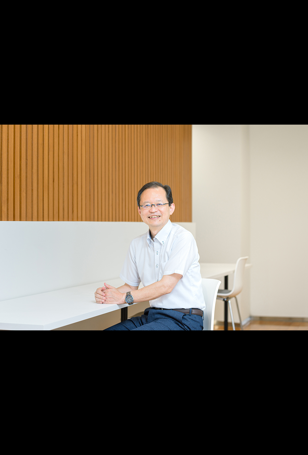
Umebayashi Taku
Sony Semiconductor Solutions Corporation
Research Division 1
Profile:Joined Sony Corporation in 1989, Umebayashi initially worked on the development of semiconductor memories, notably in preparation for the releases of the sound stuttering prevention memory for Discman and the graphic synthesizer for PS2. In 2002, he went to the USA to join the team to develop cell chips for PS3. Returning to Japan in 2005, he oversaw the launch of mass production lines for graphic chips for PS3 at the Nagasaki TEC. When reinstated at the Atsugi headquarters in 2008, he embarked on the development of stacked CMOS image sensor. He worked with a team for the development of 3-layer stacked CMOS image sensor from 2013, and since 2016 he has been in charge of the development of next-generation memory technology to be implemented on stacked CMOS image sensors.
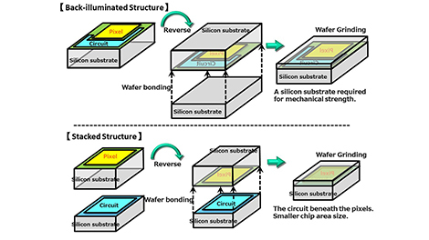
A two-layer structure—this genius could not have come from pixel design specialists
Image sensors are a semiconductor device that converts light into digital signals. They are found in many camera products such as digital cameras. An image sensor comprises pixels, that take in and convert light into electrical signals, and a logic circuit, that converts the electrical signals into digital information and processes it. Conventionally, both the pixels and logic circuit are mounted on a single chip, and it requires careful design and planning of each part in order to develop manufacturing processes to ensure one does not compromise the performance of the other. SSS those days was going strong on developing back-illuminated CMOS image sensors. This innovative device delivers high sensitivity in a low-illuminance environment by reversing the silicon substrate so that the light comes in from the back of the chip. In this way, the light receiving surface area of the pixel section can be expanded. Thanks to this key feature, SSS’s CMOS image sensors today enjoy the largest market share in the industry. So, the company was totally devoted to developing this back-illuminated CMOS image sensor, when some clients requested for a cheaper version for their mobile device products. Thus began Umebayashi’s journey to further develop the back-illuminated CMOS image sensor.
reference image
Zoom

Umebayashi spent the first month and a half going through technical articles and gathering information. Eventually he came to an idea that, in order to eliminate through the process development the chance of one component interfering with the other, they could perhaps be completely separated. He recalls, “The two-layer structure is a conclusion which I arrived at after exploring all possibilities to remove redundancies and inconsistencies in manufacturing the pixel and logic circuit sections. While the pixel section is the heart of an image sensor, I as a specialist of logic circuit saw it like a sore spot that got in the way of the logic circuit. I thought that it might work well if the components were separated and then put together after their processes were formed. In this way, both parts could fully leverage their respective advantages. Stacking the pixel section on the logic circuit section would result in a smaller chip size, and therefore the productivity per wafer would improve, which would realize a “cheaper” sensor and solve the problem.” Such an approach could only come from someone whose main focus was not on the pixel section. The idea was immediately approved, and a small project team was formed. However, he quickly came to face the first predicament, for the initial proof of concept failed so badly that it was even impossible to analyze why it failed. He had no choice but to give up on this idea. According to him, this stacked structure was so new that it was difficult to get people on board, setting a limit to what he could do. Fortunately, however, the initial failure did not end up terminating the project altogether, and he could carry on with his efforts in the development.
The most challenging part in the development was bonding between the pixel and logic circuit wafers. The wafer formed with the circuit pattern must be grinding as much and as flat as possible so that it can be layered hermetically to the pixel wafer, which was the crucial engineering to be achieved in realizing the stacked structure. The two wafers were to be electrically connected, and the connections needed to be aligned perfectly, requiring high levels of technical expertise. It was as difficult as layering two 120-meter-wide baseball grounds one on top of the other with less than 1 mm of margin of error. It took the team almost two years from the concept stage to the manufacturing of a successful sample, which in itself suggests how hard the project was. The stacked CMOS image sensor finally came into being after a long period of struggles. “The technology has come to be adopted by other manufacturers today, but it took a while since its initial market launch before they started offering products with this technology.” This is a testimony to how sophisticated the stacking technology was and how hard the development team worked on it.
A miraculous journey of the development
Positive expectations and support propelled the project to mass production
The project of stacked CMOS image sensor had another major challenge. While the separation of the two components created the possibility of mounting various additional technologies onto the logic circuit section, there was no clients chosen for this product even when the mass-production phase was in sight. Preparations were ongoing to set up mass production lines at the Kumamoto and Nagasaki Technology Center(TEC) in 2011. At this stage, however, the lack of client was stirring a skepticism as to the legitimacy of mass-producing the product. There was even a talk about suspending the development project. When the mood was one of uncertainty, the accounting division expressed their support saying, “Don't worry about the development cost which has been spent. If you think the product is good enough to recover the mass-production cost, it’s worthwhile going ahead.” Umebayashi believes that this advice boosted the morale in the team and enabled them to take the image sensor to mass production. Eventually, it was decided that the product be implemented in Xperia Z and its subsequent models, creating an opportunity for the stacked structure to be widely recognized, leading to a huge market success.
Despite numerous difficulties, the project survived to reach the mass production stage. “I believe that everyone wanted this technology to succeed. When the initial PoC failed, normally the choice would be either to end the project or replace me with someone else, but both the project and I were allowed to continue. The process team also kept trying again and again. I also learned it afterwards that my bosses were helping us behind the scenes, too, with securing the budget and making necessary arrangements for the launch of mass-production lines,” said Umebayashi, describing the strong backing the project had. “We were at our lowest toward the end of 2009. Then came 2010, the sample finally produced some image. Boy, I was so happy to see it,” he smiled. This breakthrough led to a successful sample test at the Kumamoto TEC, and the tide was turned. What started as a discrete team effort was transformed into a research work that garnered the ‘internal attention.
Logical thinking behind actions and policies
What is the source of this epochal innovation? Umebayashi says that he had a great passion for mathematics at school. “I would tackle the math textbook as soon as I got my hands on it at the beginning of a school year. I would finish it before the second term, so I would ask my math teacher to give me the textbook for higher grades.” When he was only a child, he enjoyed solving mathematical problems with his father, which gave him the impression that he was playing puzzles or quizzes. “For me, math was not a study but more like playing a game,” he recalls. Perhaps the logical thinking which he developed through mathematical training was the foundation of his idea for the streamlined stacked structure. His personal philosophy of work is “to think logically to determine my actions and policies” and “understand the outcomes in terms of the system, cause and reasoning behind them.” A developer must have an attitude like this. He says, “It is important not to speculate uncertainly and to be honest. Meanwhile, for achieving something that is technically realizable, you must be bold. If you don’t take an action, possibilities for the future may never have a chance to be tested.” His genuine and honest attitude to technology, he believes, is what enabled him to persevere almost two years of struggles to come to the major success. When he finds himself at a dead end, however, he does not hesitate to consult a few select colleagues to discuss the matter to avoid being stuck with an idea that leads to nowhere. He often finds that discussions in small groups offer him new perspectives and help to find a solution. Meanwhile, English was not his favorite subject at school. As his jobs at Sony increasingly found him in English-speaking situations such as international academic conferences, Umebayashi was seeking an opportunity to improve his command of English. His choice was to take a post in the USA. He put his name forward for the overseas assignment even though his TOEIC score did not meet the requirement for the candidacy. He “wanted to take up a new challenge” and thought it would be “an opportunity to throw myself in at the deep end, and I would have no choice but to learn English.” For Umebayashi, it was an extension of his attitude to work, a decision drawn based on his logical thinking. His experience in the USA turned out to be positive. He learned the importance of flexible thinking as he found the ways of doing things were “loose in a good sense” and that they had a totally different approach from the Japanese ways to manufacturing semiconductors.
Focus not on outcomes
but the reasons behind them
Umebayashi set his mind on a career in research and development when he was at university. He liked working in a lab, and especially, experiments more than theoretical developments. He used to run experiments with his peers, staying in the lab often until late. Finding much “fun in research,” he became determined to have this career path. However, corporate research and development was very different from the academic pursuits. While the latter focused on principles, physical interpretation and other theoretical perspectives, the former took a more pragmatic approach to the development, such as how the product should be applied, what value it added, and what needed doing to make practical applications. He also recognizes that Sony’s corporate culture that respects individual freedom has shaped his attitude to work. He says, “During my first year at Sony, I noticed that my senior colleagues did not scrutinize the research or measurements I undertook. I learned from them that it was more important to think and understand the process behind the outcomes rather than verifying the validity of the results.” There is a long-standing golden rule at Sony: If you have a good idea, pursue it without waiting for boss’ approval — if it works, make it official; if not, you can leave it there. This rule epitomizes the workplace environment that allowed Umebayashi to take up and pursue new ideas until he succeeded, and it culminated in the stacked CMOS image sensor.
He says, “It is most satisfying in my work to see the products I worked on find many users. I will continue to work on commercializing products that the world has never seen and satisfy the desire of many people.” We wish him great success in his future career.
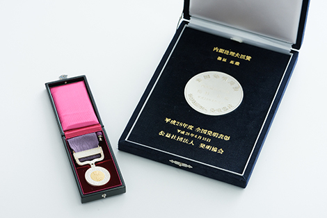
Plaques of the Prime Minister’s Award (2016 National Invention Awards) and 2020 decoration of the Medal with Purple Ribbon